Flash Lamp Annealing (FLA) was developed in the environment of the semiconductor industry. Over the course of the last years, a wide variety of application fields opened up, such as:
• thin semiconductor layers, e.g. for sensors and photovoltaics • transparent oxides, e.g. Indium-tin-oxide • energy materials, e.g. for battery technology • printed electronics • FLA-assisted deposition, e.g. flash-ALD or sputter-FLA
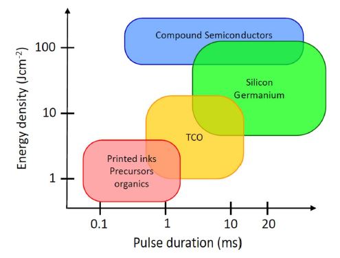
Depending on the application, the energy density (intensity), the pulse length, the repetition rate, the tempering atmosphere (air, inert gas, vacuum, etc.), the lamp arrangement and handling vary. Fig. 1 shows electrical performance parameters for typical FLA applications.
Fig.1 Electrical performance parameters for various FLA applications (according to T. Gebel et al., 10th Int. Conf. On Coatings on Glass and Plastics, S4-05 (2014))
When it comes to handling, a distinction can be made between R2R (roll-to-roll) and S2S (sheet-to-sheet) applications, in which case the substrate is usually cured as a whole using a lamp field. The following table shows a brief comparison between the two methods: