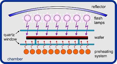
During flash lamp annealing (FLA) an energy storage is discharged via a single flash lamp or a field of flash lamps. The resulting light pulse is absorbed by the substrate or wafer and converted into heat. Fig. 1 shows the scheme of a FLA chamber. The reflector maximizes the light intensity on the front side of the substrate, while an optional pre-heating system in the back (usually a heating plate or halogen lamp) preheats the substrate. This enables higher maximum temperatures to be reached while reducing thermal stresses.
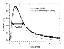
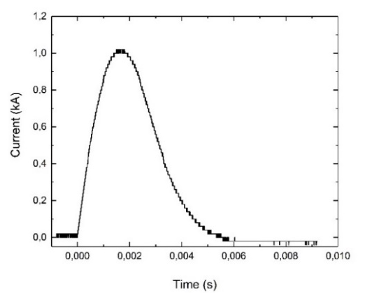
The discharge of the energy storage device generates a current pulse, which is converted into a light pulse inside the flash lamp (Fig. 2). Pulse time and pulse shape are essentially determined by the electrotechnical circuit of the energy storage device (e.g. a specific coil-capacitor combination). Typical pulse times range from a few 100 µs to a few 10 ms. The pulse time roughly corresponds to the half width at full maximum of the light or current pulse.
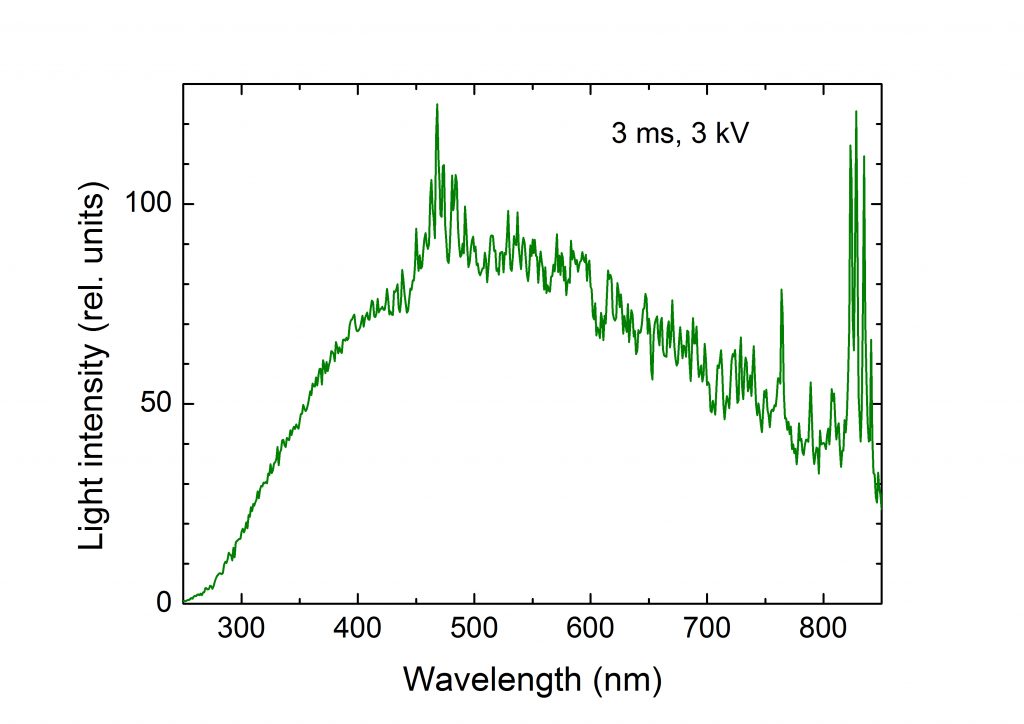
The light pulse shows a broadband spectrum from UV to the near infrared range with a maximum in the blue-green spectral range (Fig. 3). With increasing intensity of the light pulse there is a slight shift towards the UV range. In case the substrate is UV-incompatible, the UV component can be filtered out.
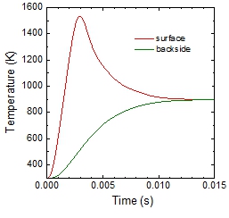
The light pulse is usually absorbed in the substrate’s near-surface regions. At the same time, the generated heat is dissipated by thermal conduction towards the backside. As a result, the temperature on the substrate surface rises, reaches a maximum value Tmax and then drops to an equilibrium value Tequ (Fig. 4). In contrast, the temperature on the backside rises continuously to Tequ. The thermal stress on the backside is therefore significantly lower than on the front side. The shorter the pulse time and the smaller the thermal conductivity of the substrate, the greater the difference between the front and backside.
Pulse shapes
In addition to various energy densities and pulse times, there are also different pulse shapes. In the normal case (a), a single pulse is applied. In the case of multi-flashing (b), several pulses with a high repetition rate are used. Depending on the energy density, repetition rates of up to 10 Hz can be realized at blitzlab. A special case is the combined pulse (c), in which two different pulses from two different charging circuitries will be added. This mode allows even higher energy densities as well as the preheating by a long pulse.