In several projects with industrial partners, the Rossendorf BlitzLab project group has successfully demonstrated millisecond annealing processes through FLA as a highly attractive technique for the functionalization of ITO layers on glass and PET [1,2] and of copper and silver paste which is used for packaging labelling by screen printing on paper-like media with a low heat budget [unpublished results].
The effect of the FLA parameters (pulse duration, energy density) on the substrate behaviour as well as on the microstructure and electrical response of the as-flashed films was studied. A significant drop of the sheet resistance of the FLA-treated layers as compared to the as printed layers was observed. As FLA permits selective, near surface heating, a damage of the sensitive substrates was avoided.
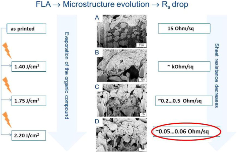
Fig. 1.: Illustration of the distinct relation between the applied annealing conditions, evolution of the sample’s microstructure and resulting sheet resistance. Material studied: Cu-film/PET, No. A) Virgin material, B) as-flashed, ED = 1.4 J/cm2, C) as-flashed, ED = 1.75 J/cm2 and D) as-flashed, ED = 2.2 J/cm2. The pulse time was 600 μs.
The microstructure of the copper paste before and after FLA was also investigated. Fig. 1 shows the correlation between the achieved sheet resistance values and the corresponding microstructure of the copper paste films. Fig.2 (left) shows an example of the positive effect of FLA on ITO glass with regard to an improvement
in the optical properties towards more transparent layers through the transition from amorphous to polycrystalline ITO layer structures, which is also accompanied by lower sheet resistance values Fig.2 (right).
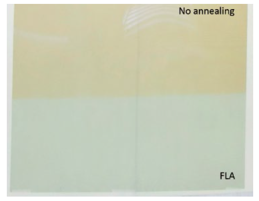
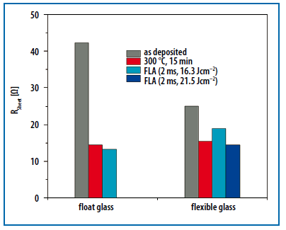
Fig. 2: Illustration of the FLA effect in relation to the optical (left) and electrical (right) properties of ITO glass layers towards more transparent and conductive layer structures (transition: amorphous polycrystalline) with significantly shorter process times (ms@FLA vs. min@oven annealing), which goes hand in hand with a more energy-efficient fabrication approach.
In the near future, our development lines will also focus on the thermal treatment of flexible or large area substrates by pulsed annealing (FLA or intense pulsed light sintering (IPL) or photonic curing). Flexible substrates demand occasionally a roll-to-roll transport system and have partly different requirements to the pulse annealing system. Normally, flexible substrates are processed in larger facilities, which comprise several processing steps like deposition, patterning and annealing. Consequently, the pulse annealing tool is integrated into the processing line as a module, see Fig. 3a [3].
Depending on the required mode of irradiation, pulsed annealing can be performed in a continuous or camera mode [1]. In continuous mode (Fig. 3b), the whole area is annealed, but between two subsequent shots there is a small overlap zone where FLA has been applied twice. If this is not acceptable, FLA can be run in camera mode (Fig. 3c) where two subsequent shots are now separated by a small, but untreated stripe.
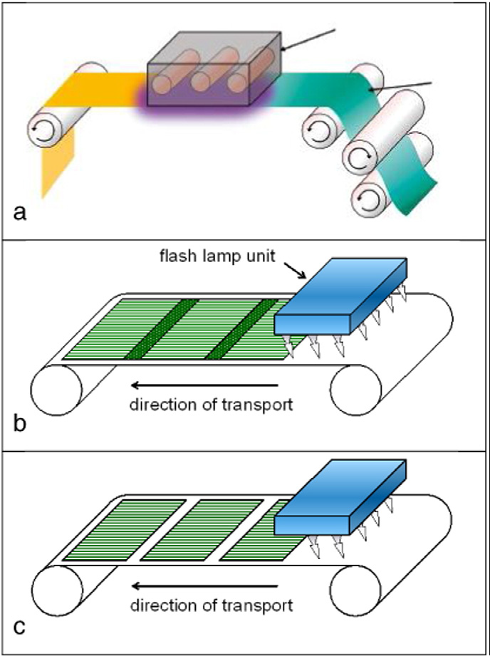
Abb. 3.: Grundschema einer FLA-Anlage für Rolle-zu-Rolle-Prozesse. (a) Copyright 2015 JohnWiley and Sons [3] FLA-Betrieb im kontinuierlichen (b) und im Kameramodus (c).
Literature:
[1] T. Gebel, L. Rebohle, R. Fendler, W. Hentsch,W. Skorupa, M. Voelskow,W. Anwand, R.A. Yankov
Millisecond annealing with flash lamps: tool and process challenges, Proc. 14th IEEE Int. Conference on Advanced Thermal Processing of Semiconductors, 2006, pp. 47–55.
[2] W. Skorupa, et al.
Millisecond beyond chip technology: from electronics to photonics, Proc. 15th IEEE Int. Conference on Advanced Thermal Processing of Semiconductors, 2007, pp. 47–55.
[3] S. Weller, M. Junghähnel
Flash lamp annealing of ITO thin films on ultra-thin glass, Vakuum in Forschung und Praxis 27 (2015) 29–33.