The ongoing miniaturization of microelectronic circuitries leads to an increasing need for alternative semiconductors with a carrier mobility strongly above this of silicon. One of these materials is germanium featuring an electron and hole mobility which are 2.5 and nearly 4 times higher than that of Si, respectively. The Processing of Ge is, inter alias, challenging for (i) achieving an n-type doping level as high as possible (ii) the fabrication of suitable contacts for n-type Ge
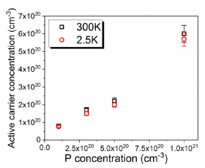
In both cases FLA is very suitable. Fig. 1 displays the active carrier concentration in phosphorous-doped Ge (n-type) after FLA as a function of the implanted phosphorous concentration. For the highest one, an active carrier concentration of 6·1020 cm-3 was achieved at an activation degree of 60%. This value is more than 3 times higher than the solubility limit of phosphorous in Ge, and cannot be realized with traditional thermal treatments (furnace, RTP).
Fig. 1: Active carrier concentration in phosphorous-doped Ge after FLA [1]
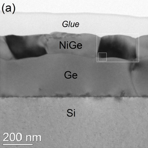
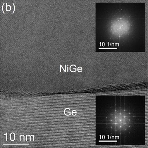
FLA can be used to fabricate a good Ohmic contact on Ge. Fig. 2 shows a TEM image of a NiGe contact on a Ge-on-insulator substrate. In the present case Ge was implanted by phosphorous, followed by the deposition of Ni. The subsequent FLA served for both the activation of dopants and the contact formation, which
reduces the number of process steps in the fabrication of Ge-based transistors. The structure displayed in Fig. 2 achieved a carrier concentration of 1·1020 cm-3 and a specific contact resistance of 1.2·10−6 Ω cm2.
Fig. 2: TEM image of a phosphorous-doped GeOI substrate with a NiGe contact after FLA (a) and detail view of the interface NiGe to Ge [2]
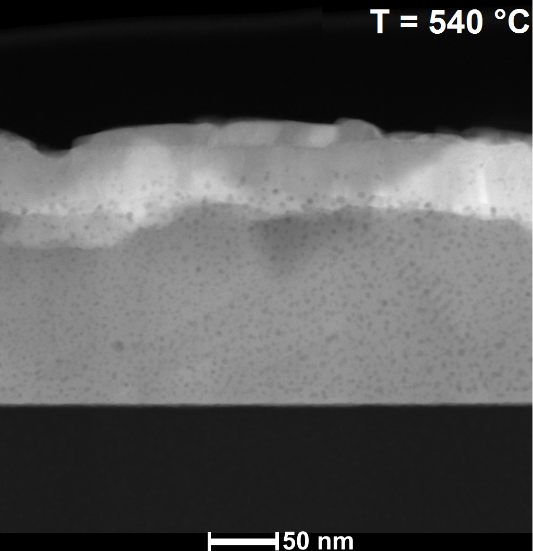
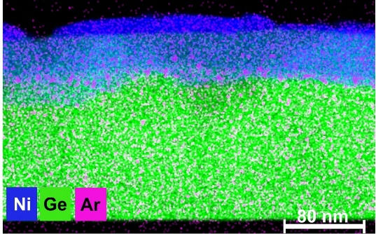
FLA is also suitable for the formation of NiGe contacts on thin, poly-crystalline Ge layers, as they are used e.g. in the field of printed or flexible electronics. Although the interface between NiGe and Ge (Fig. 3) is more diffuse compared to mono-crystalline Ge (Fig. 2),
a specific resistivity of ca. 14 µW·cm for NiGe is achieved. This value is comparable with literature values, which have been obtained by rapid thermal processing (RTP) or laser annealing.
Fig. 3: TEM image (left) and corresponding element distribution as measured by EDX (right) for 30 nm Ni on 160 nm Ge after FLA annealing.
Quellen
[1] Prucnal et al., J. Appl. Phys. 125, 245703 (2019) [2] Prucnal et al., Semicond. Sci. Technol. 32 (2017) 115006